Lesson 13.7 explained what J T A G is for and what each of its parts does. This lesson drives those parts one clock at a time, from a four-bit shift register to the packet that opens an SWD session, and ends with a lab that simulates a two-chip scan chain.
Section: Two clock edges and two default levels.
TCK is a clock: a wire that switches from 0 to 1 and back, over and over. The moment it rises from 0 to 1 is called the rising edge, and the moment it falls back to 0 is the falling edge. A J T A G chip reads TMS and TDI on the rising edge and changes TDO on the falling edge. Each wire is read on one edge and changed on the other, so no wire is ever read at the moment it changes.
The standard also requires TMS and TDI to read as 1 when nothing drives them. That small rule matters twice below.
Section: Shift registers: many bits through one wire.
J T A G’s shift registers always shift toward TDO: on each clock the cell next to TDO, bit 0, leaves first, every other bit moves down one place, and the bit arriving from TDI enters at the top.
Alternative: Picture buckets moving toward the outlet together: each tick releases one old bit and takes one new bit at the far end.
Take a small chip with four pins and a 4-bit boundary-scan register, bits b3 to b0. The test captures the pins: pin 0 reads 1, pin 1 reads 0, pin 2 reads 1, and pin 3 reads 1. Each cell now holds its own pin’s level:
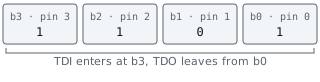
Now the debugger runs four clocks, sending 1, 1, 0, 0 into TDI, first bit first. On each clock, TDO receives b0, then b0 takes b1’s value, b1 takes b2’s, b2 takes b3’s, and b3 takes the bit from TDI:
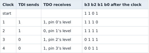
Check clock 1: TDO receives b0, which is 1. Then b0 takes b1’s 0, b1 takes b2’s 1, b2 takes b3’s 1, and b3 takes the incoming 1, giving 1 1 1 0. The other rows follow the same rule.
The same four clocks did two jobs. They read the pins out in order, pin 0 to pin 3, and they loaded a new pattern. The first bit sent travelled furthest and ended in b0; the last bit sent stopped in b3:

Look at the register after clock 2: 1 1 1 1, a pattern nobody asked for. While bits ripple through, the register passes through meaningless in-between values. If the pins followed the register directly, they would flicker through every one of them. So each cell has a second one-bit store, called a latch, that actually drives the pin, and the latch copies the shifted value only once the whole pattern is in place. That copy is the Update step of Lesson 13.7.
Section: The TAP controller: all 16 states.
Lesson 13.7 followed the main path through the TAP controller: Capture, Shift, and Update. Here is the whole machine. At every rising edge of TCK it moves to one of two next states, chosen by whether TMS is 0 or 1. The diagram writes the 16 state names without hyphens; the standard spells them Test-Logic-Reset, Run-Test/Idle, Select-DR-Scan, Capture-DR, and so on.

The machine has two matching columns. States ending in DR work on a data register, such as the boundary-scan register; states ending in IR work on the instruction register. Down each column:
Select chooses a column. With TMS at 0 it enters that column’s Capture state; with TMS at 1 it moves on, from Select-DR-Scan to Select-IR-Scan, and from Select-IR-Scan to Test-Logic-Reset.
Capture loads the register’s shift stage from its inputs: the pin levels, for the boundary-scan register.
Shift moves one bit from TDI toward TDO on every clock, for as long as TMS stays 0.
Exit1, Pause, and Exit2 leave the shifting, wait if the debugger needs time to fetch more data, and resume without starting over.
Update copies the shifted-in value to the register’s outputs in one step.
Test-Logic-Reset is the state in which the chip ignores the test logic and works normally, and Run-Test/Idle is a resting place between operations. Six states can wait in place for as long as TMS holds steady: Test-Logic-Reset with TMS at 1, and Run-Test/Idle, Shift-DR, Pause-DR, Shift-IR, and Pause-IR with TMS at 0. Every other state lasts exactly one clock.
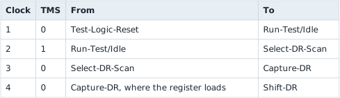
Each state does its work on the rising edge that leaves it. The capture happens on the clock that moves from Capture-DR to Shift-DR, and the last bit of a scan is shifted by the same clock that raises TMS to leave Shift-DR for Exit1-DR. To shift 64 bits, the debugger sends 63 clocks with TMS at 0 and then the 64th with TMS at 1. Getting from a fresh reset to the first shift takes four clocks:
Lesson 13.7 said that five clocks with TMS at 1 reach Test-Logic-Reset from any state. Follow the arrows labelled TMS 1 from Shift-DR, one of the states furthest away: Exit1-DR, Update-DR, Select-DR-Scan, Select-IR-Scan, and Test-Logic-Reset, which is five clocks. The reset reference below checks every other state the same way. Extra clocks do no harm, because Test-Logic-Reset stays put while TMS is 1, so a debugger that is unsure of the state sends five 1s on TMS and starts from a known place. And because an undriven TMS reads as 1, a chip whose test port is not connected to anything sits in Test-Logic-Reset permanently and works normally.
Additional detail: Optional reference: every state's path to Test-Logic-Reset.
To check the rule for all 16 states, hold TMS at 1 and work outward from Test-Logic-Reset, following the arrows labelled TMS 1:
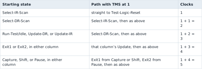
The rows cover 1 + 1 + 3 + 4 + 6 equals 15 states, and Test-Logic-Reset itself needs 0 clocks, so all 16 are accounted for and none needs more than five.
Section: BYPASS, IDCODE, and a chain that fails safe.
A few fixed rules about instruction codes shape how a debugger drives a chain.
BYPASS must be all ones, so a chip with a 4-bit instruction register uses 1111, and the one-bit register it selects always captures 0. A chip with an IDCODE register selects IDCODE on reset, so no instruction scan is needed before reading IDs.
Any code a chip does not define must behave as BYPASS. Together with the rule that an undriven TDI reads as 1, this means a broken chain fails safe: a chip whose TDI wire is cut receives nothing but ones, which select BYPASS, not a test mode that drives the pins against the chip’s own outputs.
Instructions are bits in the chain like any others. In one instruction scan the first bits shifted in travel furthest, so to give every chip its own instruction, the debugger sends the instruction for the chip nearest TDO first and the one for the chip nearest TDI last.
Section: Worked example: count the chips on a chain.
A debugger attached to an unfamiliar board can count its chips in two scans.
Reset, then shift plenty of ones through the instruction registers. The debugger does not know how long each register is, and it does not need to: every register ends up full of ones, which is BYPASS, and the spare ones fall out of TDO.
Scan the data registers. Each chip now contributes one bypass bit, which captured 0. Send a single 1 followed by 0s, and count the clocks until the 1 comes back.
Here is the second scan on a board with two chips, A nearest TDI and B nearest TDO. On each clock, TDO receives B’s bit, B takes A’s old bit, and A takes the bit from TDI:
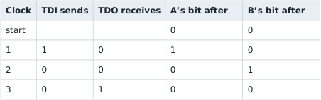
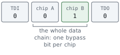
The 1 went in on clock 1 and came out on clock 3, so the chain held it for 3 minus 1 equals 2 clocks. Each one-bit register holds a bit for exactly one clock, so there are 2 chips.
Section: Reading a chip’s identity.
After reset, every chip with an IDCODE register has it selected, so one data scan reads every ID on the chain. For two chips that is 32 + 32 equals 64 bits. They come out lowest bit first, and the chip nearest TDO answers first: the first 32 bits belong to chip B.
In brief: Serial chain output begins with the chip nearest TDO, sending that selected register’s lowest bit first.
Bit 0 of every IDCODE is 1, and that is deliberate. A bypass register captures 0, so the first bit from each chip tells the debugger what kind of register it is reading. A 1 means a 32-bit IDCODE follows; a 0 means a chip with no IDCODE, sitting in BYPASS, which contributes that single bit and nothing more.
Chip A in this lesson’s lab contains Arm’s J T A G debug port, found in many microcontrollers, and it answers this value. The 32 bits split into three fields plus the fixed 1:

Bits 31 to 28 are the first hex digit: version 4.
Bits 27 to 12 are the next four digits: part number hexadecimal B A 0 0.
Bits 11 to 0 are hexadecimal 4 7 7, which is 4 times 256 + 7 times 16 + 7 equals 1,143. Its lowest bit is the fixed 1. Removing that bit means subtracting 1 and halving: (1,143 minus 1) divided by 2 equals 571. In hex, 571 equals 2 times 256 + 3 times 16 + 11 equals hexadecimal 2 3 B, the manufacturer code that JEDEC, the industry body that hands out these numbers, assigned to Arm.
Section: Halting a Cortex-M core with one write.
Arm’s Cortex-M processors keep their debug controls at fixed addresses in the memory map, and their debug logic includes a memory access port that performs bus reads and writes for the debugger. So halting the core takes one ordinary memory write through the debug port, and reading R A M, random access memory, afterwards takes one memory read. The register the halt writes is DHCSR, the Debug Halting Control and Status Register, at address shown here, described in Arm’s public architecture manual. Its low three bits are:
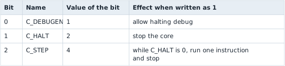
Every write must also carry hexadecimal A 0 5 F in the upper 16 bits, or the processor ignores it. That key is printed in the public manual, so it is not a password. It stops a stray write from buggy software halting the core by accident.
Narration: The public register key filters accidental writes; it is not a secret that authenticates a debugger. Its purpose follows from where and how the hardware checks it.
A 32-bit value has eight hex digits, four bits each, so its upper 16 bits are the first four digits, and putting hexadecimal A 0 5 F there gives this value. Adding bit values to it:
halt: this value + 2 + 1 equals this value;
step one instruction while halted: this value + 4 + 1 equals this value;
resume: this value + 1 equals this value.
The write travels through that memory access port. The port has an address register and a data register, called TAR and DRW in Arm’s documentation: write an address to the first, then read or write the second, and the port performs that bus access.

The second read fetches the first word of the chip’s R A M, which starts at this value on Cortex-M. Core registers come through two more memory-mapped registers, one to choose a register by number and one to carry its value.
Section: Inside an SWD request.
Lesson 13.7 showed the shape of an SWD read: an 8-bit request, a turnaround, a 3-bit acknowledgement, 32 data bits, and a parity bit. The request’s eight bits, in the order they are sent, are:
Start: always 1.
APnDP: 0 for a debug port register, 1 for an access port register.
RnW: 1 to read, 0 to write.
A2 and A3: two address bits that choose one of four registers.
Parity: makes the count of 1s among APnDP, RnW, A2, A3, and the parity bit itself even.
Stop: always 0. Park: always 1.
The first request a debugger usually sends reads the debug port’s ID register, register 0. That needs APnDP equals 0, RnW equals 1, A2 equals 0, and A3 equals 0. Those four bits contain one 1, an odd count, so the parity bit is 1, which makes two:
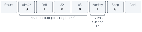
The bits in the order sent are 1, 0, 1, 0, 0, 1, 0, 1. Treating the first as bit 0, the 1s sit in bits 0, 2, 5, and 7, worth 1, 4, 32, and 128, for a total of 165. In hex that is 10 times 16 + 5 equals hexadecimal A 5.
The ID comes back in the same format as a J T A G IDCODE. For many Cortex-M chips it is this value. Split the same way as above, that is version 2, part number hexadecimal B A 0 1 for the serial-wire version of the port, and the low three digits hexadecimal 4 7 7 once again, so the same Arm manufacturer code, hexadecimal 2 3 B.
Section: Simulate a TAP controller.
The portable lab jtag_tap_lab.rs simulates the board from this lesson: chip A with Arm’s J T A G debug port, which answers this value, and a made-up sensor as chip B. No hardware is involved. The four wires are function arguments, and the board is a Vec of chips. Every chip sees the same TCK and TMS, so their controllers move in lockstep and one TapState describes them all.
The controller is a match with one row per state, giving the next state for TMS at 0 and at 1, exactly like the diagram. The shift register is five lines:
Code example. The surrounding prose explains this example; the full lesson contains the exact code.
& 1 keeps only bit 0, the bit leaving toward TDO. >> 1 moves every bit down one place. << top puts the incoming bit at the top: bit 31 for the IDCODE register, or bit 0 for the one-bit bypass register, where the top and the bottom are the same cell. The chain passes each chip’s outgoing bit into the next chip:
Code example. The surrounding prose explains this example; the full lesson contains the exact code.
Build it, then run it from the rust-labs folder:
Terminal window
Code example. The surrounding prose explains this example; the full lesson contains the exact code.
The lab walks from Shift-DR to Test-Logic-Reset in five clocks and confirms that no state needs more. It reads both IDCODEs, chip B’s first because chip B is nearest TDO, and splits Arm’s into the fields above. It counts the chips by timing a single 1 through their bypass bits. Finally, it puts chip A on IDCODE and chip B on BYPASS, which makes the data chain 32 + 1 equals 33 bits long. The tests check that every state resets within five clocks, that exactly six states can wait in place, that undefined instructions behave as BYPASS, and that instructions land in chain order.
Then add a third chip to board(). Before you run it, predict what count_chips reports and how many bits the IDCODE scan in main now needs.